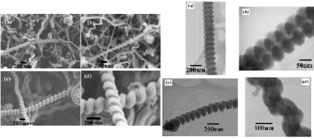
 The image on the left is a montage of FESEM snapshots of mats of silica nanosprings and closeup views of individual nanosprings within the mat. The image on the right is a montage of TEM snapshots of individual silica nanosprings.
The process for creating silica nanosprings was developed in our laboratory at the University of Idaho in 2005. We consider this to be a breakthrough for the following reasons: The process conditions are atmospheric pressure and a growth temperature as low as 325 C, as opposed to vacuum conditions and ~1000 C for boron carbide and silicon carbide nanosprings. The process is as short as fifteen minutes, as opposed to hours for boron carbide and silicon carbide, i.e. the growth rate is very fast due to the atmospheric pressure of the precursor materials. Last, but not least, we can make of lot of them. Currently, we can produce approximately 350 mg of nanosprings in one run.
 Above is a picture of our stash of nanosprings lying around in the lab. We can grow them on virtually any surface.
If you are interested in collaborating on a project using nanosprings drop me an email at dave.mcilroy@okstate.edu.